

Section 01 · 6 lectures
Introduction
Why nanoelectronics is worth modelling, and what a model has to get right: the numbers behind the scaling of the transistor, a channel small enough that its atoms can be counted, the band structure a device engineer needs, a pn junction solved with drift-diffusion, the three small apps that stand in for the nanoHUB tools, and the open problems NEMO was written for.
Lecture 1.1
Why are nanoelectronic devices interesting?
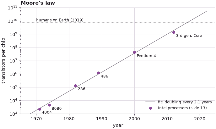
put the lecture's numbers into a few lines of code (the Cray-2/iPad ratios, the doubling time of the transistor count, the yearly fall of the price per transistor), then use open-nemo to build the 8 nm silicon fin's crystal
Interactive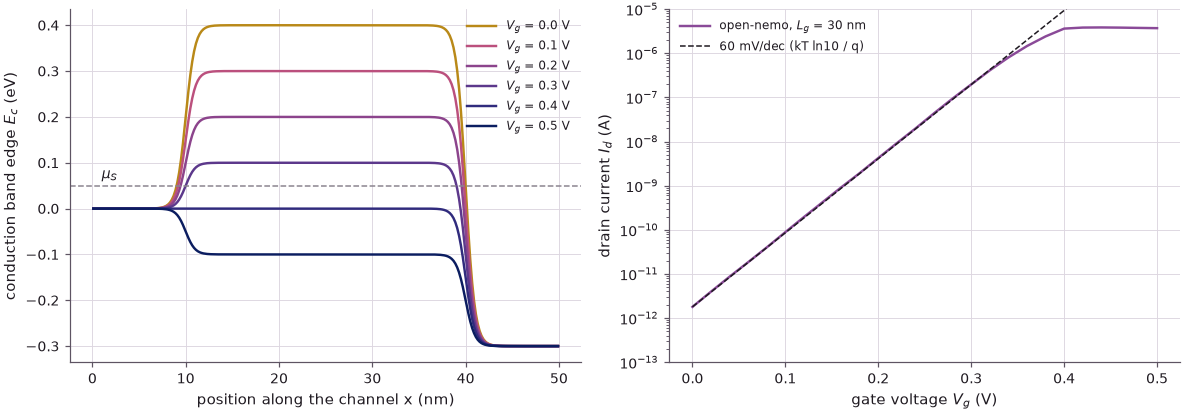
Lecture 1.2
Basic device operation — raising 1,000 questions
turn the slide pictures into calculations. A one-dimensional effective-mass model of the channel (a barrier whose height the gate sets, ballistic transmission from open-nemo's Transport
Lecture 1.3
Band structure in nanoelectronics — a basic view
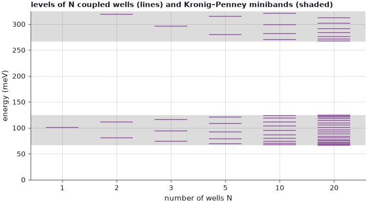
compute each picture. Coupled quantum wells in open-nemo show discrete levels turning into a band, checked against the Kronig–Penney formula
Interactive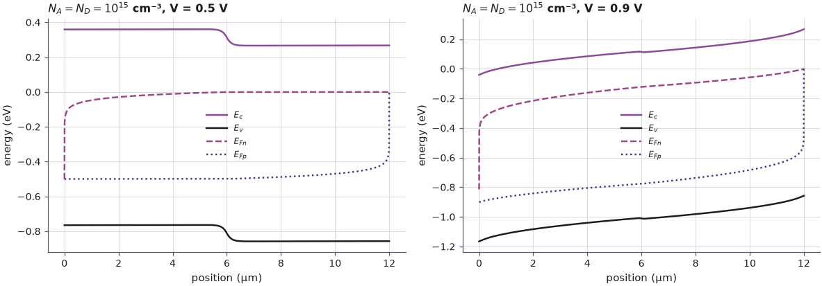
Lecture 1.4
Use of simulation to explain concepts — PN junction to device scaling
repeat the pn-junction exploration of the slides with a small drift–diffusion simulator: open-nemo's nonlinear Poisson solver for the electrostatic potential and a few lines of numpy for
Interactive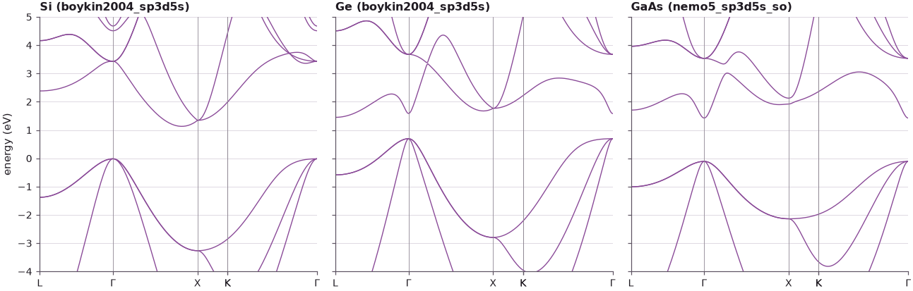
Lecture 1.5
nanoHUB access and tool demo
do the tool demonstration with open-nemo's three small apps, the ones behind its interactive explorer: the bulk band structure of a crystal, the ballistic transmission of a silicon nanowire
Interactive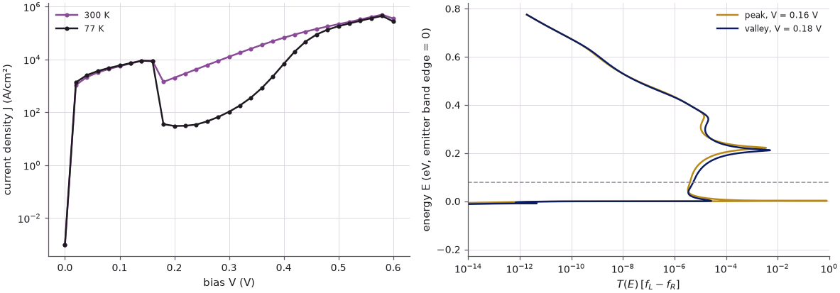
Lecture 2
Challenges at the frontier of quantum transport modeling (NEMO and nanoHUB)
compute small versions of the lecture's key results with open-nemo: the atom counts of the technology nodes; a non-equilibrium Green's function calculation written out by hand and compared with open-nemo's transport solver
Interactive